
A English
PN Junction and Diode Questions in English
Class 12 Physics · Semiconductor Electronics · PN Junction and Diode
415+
Questions
English
Language
100%
With Solutions
Showing 15 of 415 questions in English
401
MediumMCQ
In a semiconductor $p-n$ diode, the doping concentrations on $p$-side and $n$-side are $10^{15} \text{ atoms/cm}^3$ and $10^{18} \text{ atoms/cm}^3$, respectively. Which one of the following statements is true?
A
Widths of depletion region on either side of the interface are equal
B
The depletion region width is more on $p$-side compared to that in $n$-side
C
The depletion region width is more on $n$-side compared to that in $p$-side
D
No depletion region forms because of unequal doping concentrations on $p$ and $n$-sides
Solution
(B) The width of the depletion region $(w)$ in a $p-n$ junction is inversely proportional to the doping concentration $(N)$ on that side, expressed as $w \propto 1/N$.
Given that the $p$-side has a lower doping concentration $(10^{15} \text{ atoms/cm}^3)$ compared to the $n$-side $(10^{18} \text{ atoms/cm}^3)$, the depletion region will extend further into the $p$-side.
Therefore, the depletion region width is greater on the $p$-side than on the $n$-side.
Given that the $p$-side has a lower doping concentration $(10^{15} \text{ atoms/cm}^3)$ compared to the $n$-side $(10^{18} \text{ atoms/cm}^3)$, the depletion region will extend further into the $p$-side.
Therefore, the depletion region width is greater on the $p$-side than on the $n$-side.
0 likes
View Solution402
DifficultMCQ
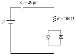
Consider a circuit consisting of a capacitor $(20 \mu\text{F})$, a resistor $(100 \Omega)$, and two identical diodes as shown in the figure. The resistance of each diode under forward biasing condition is $10 \Omega$. The time constant of the circuit is $\alpha \times 10^{-3} \text{ s}$. The value of $\alpha$ is . . . . . . .
A
$2.2$
B
$2$
C
$2.1$
D
$2.4$
Solution
(C) The time constant of an $RC$ circuit is given by $\tau = R_{eq}C$.
In the given circuit, there is a resistor $R = 100 \Omega$ in series with a parallel combination of two identical diodes.
Each diode has a resistance of $10 \Omega$ in the forward bias condition.
The equivalent resistance of the two diodes in parallel is $R_d = \frac{10 \times 10}{10 + 10} = 5 \Omega$.
The total resistance of the circuit is $R_{total} = R + R_d = 100 \Omega + 5 \Omega = 105 \Omega$.
The capacitance is $C = 20 \mu\text{F} = 20 \times 10^{-6} \text{ F}$.
Thus, the time constant $\tau = R_{total} \times C = 105 \Omega \times 20 \times 10^{-6} \text{ F} = 2100 \times 10^{-6} \text{ s} = 2.1 \times 10^{-3} \text{ s}$.
Comparing this with $\alpha \times 10^{-3} \text{ s}$, we get $\alpha = 2.1$.
In the given circuit, there is a resistor $R = 100 \Omega$ in series with a parallel combination of two identical diodes.
Each diode has a resistance of $10 \Omega$ in the forward bias condition.
The equivalent resistance of the two diodes in parallel is $R_d = \frac{10 \times 10}{10 + 10} = 5 \Omega$.
The total resistance of the circuit is $R_{total} = R + R_d = 100 \Omega + 5 \Omega = 105 \Omega$.
The capacitance is $C = 20 \mu\text{F} = 20 \times 10^{-6} \text{ F}$.
Thus, the time constant $\tau = R_{total} \times C = 105 \Omega \times 20 \times 10^{-6} \text{ F} = 2100 \times 10^{-6} \text{ s} = 2.1 \times 10^{-3} \text{ s}$.
Comparing this with $\alpha \times 10^{-3} \text{ s}$, we get $\alpha = 2.1$.
0 likes
View Solution403
MediumMCQ
Two statements are given below:
$A$. When the forward bias voltage across a $p-n$ junction diode increases above a certain threshold voltage, the diode current increases significantly.
$B$. This current is called reverse saturation current.
Choose the correct answer from the options given below:
$A$. When the forward bias voltage across a $p-n$ junction diode increases above a certain threshold voltage, the diode current increases significantly.
$B$. This current is called reverse saturation current.
Choose the correct answer from the options given below:
A
Both Statements $A$ and $B$ are true
B
Both Statements $A$ and $B$ are false
C
Statement $A$ is true, but Statement $B$ is false
D
Statement $A$ is false, but Statement $B$ is true
Solution
(C) Statement $A$ is correct: In a $p-n$ junction, forward bias reduces the potential barrier, allowing current to rise sharply after the threshold voltage.
Statement $B$ is incorrect: The current in forward bias is called forward current. The term 'reverse saturation current' refers to the very small, nearly constant current that flows in a $p-n$ junction diode when it is in reverse bias.
Therefore, Statement $A$ is true and Statement $B$ is false.
Statement $B$ is incorrect: The current in forward bias is called forward current. The term 'reverse saturation current' refers to the very small, nearly constant current that flows in a $p-n$ junction diode when it is in reverse bias.
Therefore, Statement $A$ is true and Statement $B$ is false.
0 likes
View Solution404
MediumMCQ
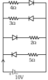
The current $I$ in the circuit shown below is: (All diodes are ideal and identical)
A
$\frac{1}{3} \text{A}$
B
$\frac{15}{2} \text{A}$
C
$\frac{5}{3} \text{A}$
D
$\frac{5}{9} \text{A}$
Solution
(B) The circuit consists of four parallel branches connected to a $10 \text{V}$ $DC$ source.
Each branch contains a resistor and a diode.
Analyzing the polarity of the diodes with respect to the $10 \text{V}$ battery:
$1$. The top branch ($4 \Omega$ resistor) has the diode in forward-biased condition.
$2$. The second branch ($3 \Omega$ resistor) has the diode in reverse-biased condition (it acts as an open circuit).
$3$. The third branch ($2 \Omega$ resistor) has the diode in forward-biased condition.
$4$. The bottom branch ($5 \Omega$ resistor) has the diode in reverse-biased condition (it acts as an open circuit).
Only the branches with $4 \Omega$ and $2 \Omega$ resistors are active.
These two resistors are in parallel, so the equivalent resistance $R_{\text{eq}}$ is:
$R_{\text{eq}} = \frac{4 \times 2}{4 + 2} = \frac{8}{6} = \frac{4}{3} \Omega$.
The total current $I$ drawn from the battery is:
$I = \frac{V}{R_{\text{eq}}} = \frac{10}{4/3} = \frac{30}{4} = 7.5 \text{A} = \frac{15}{2} \text{A}$.
Thus, the correct option is $B$.
Each branch contains a resistor and a diode.
Analyzing the polarity of the diodes with respect to the $10 \text{V}$ battery:
$1$. The top branch ($4 \Omega$ resistor) has the diode in forward-biased condition.
$2$. The second branch ($3 \Omega$ resistor) has the diode in reverse-biased condition (it acts as an open circuit).
$3$. The third branch ($2 \Omega$ resistor) has the diode in forward-biased condition.
$4$. The bottom branch ($5 \Omega$ resistor) has the diode in reverse-biased condition (it acts as an open circuit).
Only the branches with $4 \Omega$ and $2 \Omega$ resistors are active.
These two resistors are in parallel, so the equivalent resistance $R_{\text{eq}}$ is:
$R_{\text{eq}} = \frac{4 \times 2}{4 + 2} = \frac{8}{6} = \frac{4}{3} \Omega$.
The total current $I$ drawn from the battery is:
$I = \frac{V}{R_{\text{eq}}} = \frac{10}{4/3} = \frac{30}{4} = 7.5 \text{A} = \frac{15}{2} \text{A}$.
Thus, the correct option is $B$.
0 likes
View Solution405
MediumMCQ
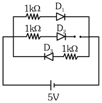
Three identical p-n junction diodes $D_1$, $D_2$ and $D_3$ are connected across a battery as shown in the figure. If the widths of the depletion regions of $D_1$, $D_2$ and $D_3$ are $W_1$, $W_2$ and $W_3$, respectively, then the correct option is:
A
$W_1 > W_2 > W_3$
B
$W_3 = W_1 > W_2$
C
$W_3 > W_2 > W_1$
D
$W_2 > W_1 = W_3$
Solution
(C) $1$. Analyze the biasing of each diode:
- Diode $D_1$ is forward-biased because its p-side is connected to the positive terminal of the battery.
- Diode $D_2$ is in an open circuit (due to the gap in the wire), so no current flows through it. It acts as an unbiased diode.
- Diode $D_3$ is reverse-biased because its n-side is connected to the positive terminal of the battery.
$2$. Relate bias to depletion width:
- Forward bias reduces the depletion width $(W_f < W_0)$.
- Unbiased state has a standard depletion width $(W_0)$.
- Reverse bias increases the depletion width $(W_r > W_0)$.
$3$. Compare the widths:
- For $D_1$ (forward-biased): $W_1$ is minimum.
- For $D_2$ (unbiased): $W_2$ is intermediate.
- For $D_3$ (reverse-biased): $W_3$ is maximum.
Therefore, $W_3 > W_2 > W_1$.
- Diode $D_1$ is forward-biased because its p-side is connected to the positive terminal of the battery.
- Diode $D_2$ is in an open circuit (due to the gap in the wire), so no current flows through it. It acts as an unbiased diode.
- Diode $D_3$ is reverse-biased because its n-side is connected to the positive terminal of the battery.
$2$. Relate bias to depletion width:
- Forward bias reduces the depletion width $(W_f < W_0)$.
- Unbiased state has a standard depletion width $(W_0)$.
- Reverse bias increases the depletion width $(W_r > W_0)$.
$3$. Compare the widths:
- For $D_1$ (forward-biased): $W_1$ is minimum.
- For $D_2$ (unbiased): $W_2$ is intermediate.
- For $D_3$ (reverse-biased): $W_3$ is maximum.
Therefore, $W_3 > W_2 > W_1$.
0 likes
View Solution406
MediumMCQ
For a $p-n$ junction diode, breakdown voltage occurs when
A
reverse bias is decreased
B
reverse bias is not changed
C
reverse-bias is increased
D
forward bias is increased
Solution
(C) In a $p-n$ junction diode, the depletion region width increases with an increase in reverse bias voltage.
When the reverse bias voltage is increased to a critical value known as the breakdown voltage, the electric field across the junction becomes very strong.
This strong electric field causes a large number of charge carriers to be generated (either through Zener breakdown or Avalanche breakdown), leading to a sudden increase in the reverse current.
Therefore, breakdown occurs when the reverse bias is increased to this critical value.
When the reverse bias voltage is increased to a critical value known as the breakdown voltage, the electric field across the junction becomes very strong.
This strong electric field causes a large number of charge carriers to be generated (either through Zener breakdown or Avalanche breakdown), leading to a sudden increase in the reverse current.
Therefore, breakdown occurs when the reverse bias is increased to this critical value.
0 likes
View Solution407
MediumMCQ
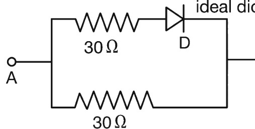
In the diagram shown, the resistance between points $A$ and $B$ is '$R_1$' when an ideal diode $D$ is forward biased and is '$R_2$' when ideal diode $D$ is reverse biased. The ratio $R_1/R_2$ is
A
$2$
B
$1$
C
$1/2$
D
$1/4$
Solution
(C) An ideal diode in forward bias acts as a short circuit (zero resistance), and in reverse bias, it acts as an open circuit (infinite resistance).
Case $1$: Diode $D$ is forward biased.
The upper branch has a resistance of $30 \ \Omega$ in series with the diode (which acts as $0 \ \Omega$). The lower branch has a resistance of $30 \ \Omega$. These two branches are in parallel.
$R_1 = (30 \ \Omega \parallel 30 \ \Omega) = \frac{30 \times 30}{30 + 30} = \frac{900}{60} = 15 \ \Omega$.
Case $2$: Diode $D$ is reverse biased.
The upper branch acts as an open circuit (infinite resistance). Thus, only the lower branch with $30 \ \Omega$ resistance is connected between $A$ and $B$.
$R_2 = 30 \ \Omega$.
Ratio $R_1/R_2 = 15/30 = 1/2$.
Case $1$: Diode $D$ is forward biased.
The upper branch has a resistance of $30 \ \Omega$ in series with the diode (which acts as $0 \ \Omega$). The lower branch has a resistance of $30 \ \Omega$. These two branches are in parallel.
$R_1 = (30 \ \Omega \parallel 30 \ \Omega) = \frac{30 \times 30}{30 + 30} = \frac{900}{60} = 15 \ \Omega$.
Case $2$: Diode $D$ is reverse biased.
The upper branch acts as an open circuit (infinite resistance). Thus, only the lower branch with $30 \ \Omega$ resistance is connected between $A$ and $B$.
$R_2 = 30 \ \Omega$.
Ratio $R_1/R_2 = 15/30 = 1/2$.
0 likes
View Solution408
DifficultMCQ
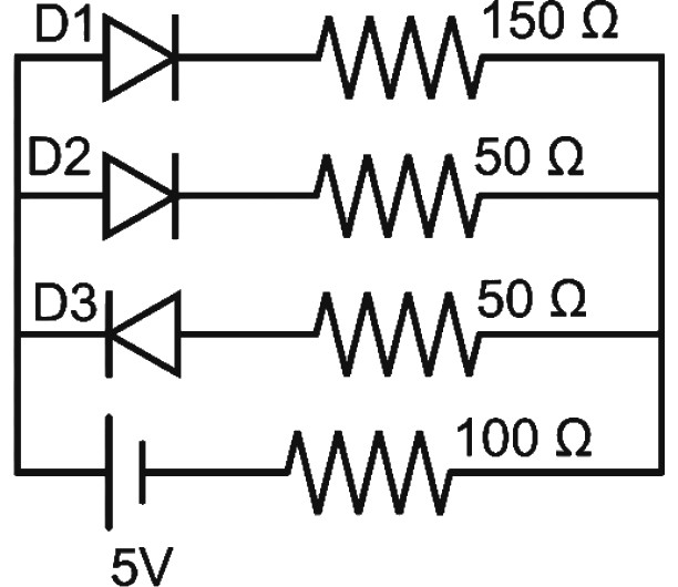
In the circuit, all three diodes $D_1, D_2, D_3$ have a forward resistance of $50 \text{ } \Omega$ each and infinite backward resistance. If the battery voltage is $5 \text{ V}$, find the current through the $100 \text{ } \Omega$ resistance. (in $\text{mA}$)
A
$60$
B
$30$
C
$20$
D
$10$
Solution
(B) $1$. Analyze the circuit: The diodes $D_1$ and $D_2$ are forward-biased, while $D_3$ is reverse-biased.
$2$. Since $D_3$ is reverse-biased, it acts as an open circuit (infinite resistance), so no current flows through the branch containing $D_3$.
$3$. The circuit simplifies to two parallel branches connected in series with the $100 \text{ } \Omega$ resistor.
$4$. Branch $1$ (containing $D_1$): Total resistance $R_1 = R_{D1} + 150 \text{ } \Omega = 50 \text{ } \Omega + 150 \text{ } \Omega = 200 \text{ } \Omega$.
$5$. Branch $2$ (containing $D_2$): Total resistance $R_2 = R_{D2} + 50 \text{ } \Omega = 50 \text{ } \Omega + 50 \text{ } \Omega = 100 \text{ } \Omega$.
$6$. The equivalent resistance of the parallel combination of $R_1$ and $R_2$ is $R_p = \frac{R_1 \times R_2}{R_1 + R_2} = \frac{200 \times 100}{200 + 100} = \frac{20000}{300} = \frac{200}{3} \text{ } \Omega$.
$7$. The total resistance of the circuit is $R_{total} = R_p + 100 \text{ } \Omega = \frac{200}{3} + 100 = \frac{500}{3} \text{ } \Omega$.
$8$. The total current $I$ flowing from the battery is $I = \frac{V}{R_{total}} = \frac{5}{500/3} = \frac{15}{500} = 0.03 \text{ A} = 30 \text{ mA}$.
$2$. Since $D_3$ is reverse-biased, it acts as an open circuit (infinite resistance), so no current flows through the branch containing $D_3$.
$3$. The circuit simplifies to two parallel branches connected in series with the $100 \text{ } \Omega$ resistor.
$4$. Branch $1$ (containing $D_1$): Total resistance $R_1 = R_{D1} + 150 \text{ } \Omega = 50 \text{ } \Omega + 150 \text{ } \Omega = 200 \text{ } \Omega$.
$5$. Branch $2$ (containing $D_2$): Total resistance $R_2 = R_{D2} + 50 \text{ } \Omega = 50 \text{ } \Omega + 50 \text{ } \Omega = 100 \text{ } \Omega$.
$6$. The equivalent resistance of the parallel combination of $R_1$ and $R_2$ is $R_p = \frac{R_1 \times R_2}{R_1 + R_2} = \frac{200 \times 100}{200 + 100} = \frac{20000}{300} = \frac{200}{3} \text{ } \Omega$.
$7$. The total resistance of the circuit is $R_{total} = R_p + 100 \text{ } \Omega = \frac{200}{3} + 100 = \frac{500}{3} \text{ } \Omega$.
$8$. The total current $I$ flowing from the battery is $I = \frac{V}{R_{total}} = \frac{5}{500/3} = \frac{15}{500} = 0.03 \text{ A} = 30 \text{ mA}$.
0 likes
View Solution409
MediumMCQ
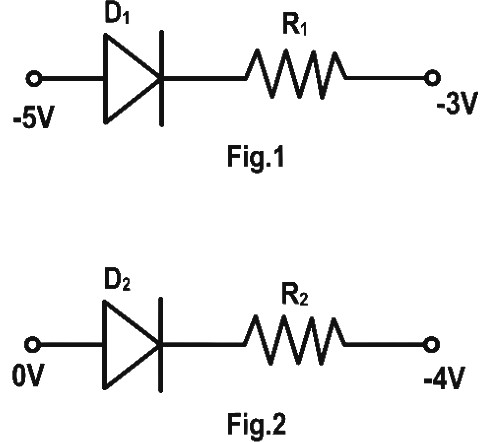
$A$ diode and a resistor are connected as shown in the figure. Out of the following statements, which one is true regarding the biasing of the diodes?
A
Fig. $(1)$ and Fig. $(2)$ are both forward biased.
B
Fig. $(1)$ and Fig. $(2)$ are both reverse biased.
C
Fig. $(1)$ is forward biased and Fig. $(2)$ is reverse biased.
D
Fig. $(1)$ is reverse biased and Fig. $(2)$ is forward biased.
Solution
(D) diode is forward biased if the potential at the $p$-side (anode) is higher than the potential at the $n$-side (cathode). Otherwise, it is reverse biased.
In Fig. $(1)$:
The $p$-side of diode $D_1$ is at $-5 \ V$ and the $n$-side is connected to $-3 \ V$ through resistor $R_1$. Since $-5 \ V < -3 \ V$, the potential at the $p$-side is lower than the potential at the $n$-side. Therefore, diode $D_1$ is reverse biased.
In Fig. $(2)$:
The $p$-side of diode $D_2$ is at $0 \ V$ and the $n$-side is connected to $-4 \ V$ through resistor $R_2$. Since $0 \ V > -4 \ V$, the potential at the $p$-side is higher than the potential at the $n$-side. Therefore, diode $D_2$ is forward biased.
Thus, Fig. $(1)$ is reverse biased and Fig. $(2)$ is forward biased.
In Fig. $(1)$:
The $p$-side of diode $D_1$ is at $-5 \ V$ and the $n$-side is connected to $-3 \ V$ through resistor $R_1$. Since $-5 \ V < -3 \ V$, the potential at the $p$-side is lower than the potential at the $n$-side. Therefore, diode $D_1$ is reverse biased.
In Fig. $(2)$:
The $p$-side of diode $D_2$ is at $0 \ V$ and the $n$-side is connected to $-4 \ V$ through resistor $R_2$. Since $0 \ V > -4 \ V$, the potential at the $p$-side is higher than the potential at the $n$-side. Therefore, diode $D_2$ is forward biased.
Thus, Fig. $(1)$ is reverse biased and Fig. $(2)$ is forward biased.
0 likes
View Solution410
DifficultMCQ
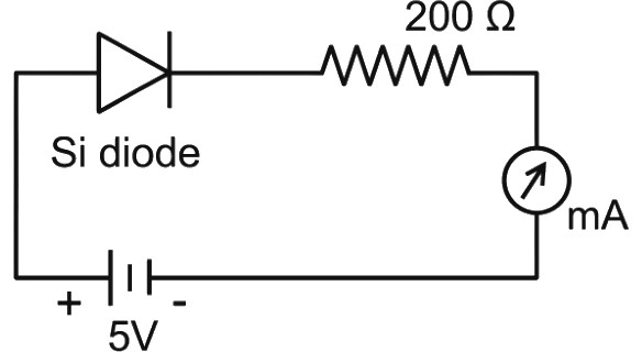
In the following electrical circuit, the reading in the milliammeter is (Take knee voltage of silicon diode $= 0.7 \text{ V}$) (in $\text{ mA}$)
A
$25.5$
B
$21.5$
C
$18.5$
D
$15.8$
Solution
(B) The given circuit consists of a $5 \text{ V}$ $DC$ source, a silicon diode, and a resistor of $200 \text{ } \Omega$ connected in series.
Since the diode is forward-biased, it will conduct current when the applied voltage exceeds its knee voltage.
The effective voltage across the resistor $(V_R)$ is given by:
$V_R = V_{\text{source}} - V_{\text{knee}}$
$V_R = 5 \text{ V} - 0.7 \text{ V} = 4.3 \text{ V}$
Using Ohm's law, the current $(I)$ flowing through the circuit is:
$I = \frac{V_R}{R}$
$I = \frac{4.3 \text{ V}}{200 \text{ } \Omega} = 0.0215 \text{ A}$
To convert the current into milliamperes (mA):
$I = 0.0215 \times 1000 \text{ mA} = 21.5 \text{ mA}$
Therefore, the reading in the milliammeter is $21.5 \text{ mA}$.
Since the diode is forward-biased, it will conduct current when the applied voltage exceeds its knee voltage.
The effective voltage across the resistor $(V_R)$ is given by:
$V_R = V_{\text{source}} - V_{\text{knee}}$
$V_R = 5 \text{ V} - 0.7 \text{ V} = 4.3 \text{ V}$
Using Ohm's law, the current $(I)$ flowing through the circuit is:
$I = \frac{V_R}{R}$
$I = \frac{4.3 \text{ V}}{200 \text{ } \Omega} = 0.0215 \text{ A}$
To convert the current into milliamperes (mA):
$I = 0.0215 \times 1000 \text{ mA} = 21.5 \text{ mA}$
Therefore, the reading in the milliammeter is $21.5 \text{ mA}$.
0 likes
View Solution411
MediumMCQ
The depletion region of a $p-n$ junction:
A
increases if reverse biased.
B
increases if forward biased.
C
decreases if reverse biased.
D
remains same in reverse and forward biasing.
Solution
(A) In a $p-n$ junction, the depletion region is formed by the diffusion of charge carriers across the junction.
When the junction is forward biased, the external electric field opposes the internal electric field, which pushes the charge carriers towards the junction, thereby decreasing the width of the depletion region.
When the junction is reverse biased, the external electric field supports the internal electric field, which pulls the charge carriers away from the junction, thereby increasing the width of the depletion region.
Therefore, the depletion region increases if the junction is reverse biased.
When the junction is forward biased, the external electric field opposes the internal electric field, which pushes the charge carriers towards the junction, thereby decreasing the width of the depletion region.
When the junction is reverse biased, the external electric field supports the internal electric field, which pulls the charge carriers away from the junction, thereby increasing the width of the depletion region.
Therefore, the depletion region increases if the junction is reverse biased.
0 likes
View Solution412
MediumMCQ
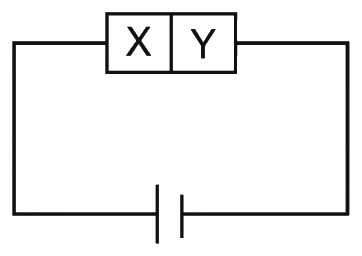
$A$ semiconductor $X$ is made by doping a germanium crystal with indium $(Z = 49)$. $A$ second semiconductor $Y$ is made by doping germanium crystal with arsenic $(Z = 33)$. Both are joined end to end and connected to a battery as shown. Which of the following statements is correct?
A
$X$ is p-type, $Y$ is n-type and the junction is forward biased.
B
$X$ is p-type, $Y$ is n-type and the junction is reverse biased.
C
$X$ is n-type, $Y$ is p-type and the junction is forward biased.
D
$X$ is n-type, $Y$ is p-type and the junction is reverse biased.
Solution
(B) $1$. Germanium $(Ge)$ is a group $14$ element. Indium $(In)$ is a group $13$ element. Doping $Ge$ with $In$ creates a p-type semiconductor. Thus, $X$ is p-type.
$2$. Arsenic $(As)$ is a group $15$ element. Doping $Ge$ with $As$ creates an n-type semiconductor. Thus, $Y$ is n-type.
$3$. The junction formed is a p-n junction.
$4$. In the circuit diagram, the p-side $(X)$ is connected to the negative terminal of the battery and the n-side $(Y)$ is connected to the positive terminal of the battery.
$5$. When the p-side is connected to the negative terminal and the n-side is connected to the positive terminal, the p-n junction is reverse biased.
$2$. Arsenic $(As)$ is a group $15$ element. Doping $Ge$ with $As$ creates an n-type semiconductor. Thus, $Y$ is n-type.
$3$. The junction formed is a p-n junction.
$4$. In the circuit diagram, the p-side $(X)$ is connected to the negative terminal of the battery and the n-side $(Y)$ is connected to the positive terminal of the battery.
$5$. When the p-side is connected to the negative terminal and the n-side is connected to the positive terminal, the p-n junction is reverse biased.
0 likes
View Solution413
MediumMCQ
If a $p-n$ junction diode is forward biased, then:
A
width of depletion layer decreases.
B
width of depletion layer increases.
C
barrier voltage increases.
D
electric conduction is not possible.
Solution
(A) When a $p-n$ junction diode is forward biased, the positive terminal of the external battery is connected to the $p$-type region and the negative terminal to the $n$-type region.
This external electric field opposes the internal electric field of the depletion region.
As a result, the majority charge carriers are pushed towards the junction, which reduces the width of the depletion layer.
Consequently, the potential barrier height decreases, allowing current to flow through the diode.
This external electric field opposes the internal electric field of the depletion region.
As a result, the majority charge carriers are pushed towards the junction, which reduces the width of the depletion layer.
Consequently, the potential barrier height decreases, allowing current to flow through the diode.
0 likes
View Solution414
MediumMCQ
In which of the following figures is the diode reverse biased?
A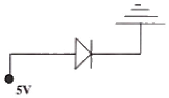
B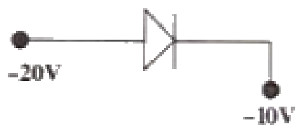
C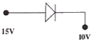
D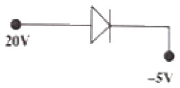
Solution
(B) diode is reverse biased when the potential at the $p$-terminal (anode) is lower than the potential at the $n$-terminal (cathode).
$(1)$ $p$-terminal = $5 \text{ V}$, $n$-terminal = $0 \text{ V}$ (ground). Since $5 \text{ V} > 0 \text{ V}$, it is forward biased.
$(2)$ $p$-terminal = $-20 \text{ V}$, $n$-terminal = $-10 \text{ V}$. Since $-20 \text{ V} < -10 \text{ V}$, it is reverse biased.
$(3)$ $p$-terminal = $15 \text{ V}$, $n$-terminal = $10 \text{ V}$. Since $15 \text{ V} > 10 \text{ V}$, it is forward biased.
$(4)$ $p$-terminal = $20 \text{ V}$, $n$-terminal = $-5 \text{ V}$. Since $20 \text{ V} > -5 \text{ V}$, it is forward biased.
Thus, the diode is reverse biased in Figure $(2)$.
$(1)$ $p$-terminal = $5 \text{ V}$, $n$-terminal = $0 \text{ V}$ (ground). Since $5 \text{ V} > 0 \text{ V}$, it is forward biased.
$(2)$ $p$-terminal = $-20 \text{ V}$, $n$-terminal = $-10 \text{ V}$. Since $-20 \text{ V} < -10 \text{ V}$, it is reverse biased.
$(3)$ $p$-terminal = $15 \text{ V}$, $n$-terminal = $10 \text{ V}$. Since $15 \text{ V} > 10 \text{ V}$, it is forward biased.
$(4)$ $p$-terminal = $20 \text{ V}$, $n$-terminal = $-5 \text{ V}$. Since $20 \text{ V} > -5 \text{ V}$, it is forward biased.
Thus, the diode is reverse biased in Figure $(2)$.
0 likes
View Solution415
MediumMCQ
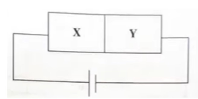
$A$ wafer of pure germanium crystal has two parts $X$ and $Y$. The end $X$ is obtained by doping with arsenic and $Y$ with indium. It is connected to a battery as shown in the figure. Which of the following statements is correct?
A
$X$ is $p$-type, $Y$ is $n$-type and the junction is forward biased
B
$X$ is $n$-type, $Y$ is $p$-type and the junction is forward biased
C
$X$ is $p$-type, $Y$ is $n$-type and the junction is reverse biased
D
$X$ is $n$-type, $Y$ is $p$-type and the junction is reverse biased
Solution
(D) $1$. Arsenic $(As)$ is a pentavalent impurity. Doping germanium with arsenic creates an $n$-type semiconductor. Thus, $X$ is $n$-type.
$2$. Indium $(In)$ is a trivalent impurity. Doping germanium with indium creates a $p$-type semiconductor. Thus, $Y$ is $p$-type.
$3$. In the circuit diagram, the positive terminal of the battery is connected to $X$ ($n$-type) and the negative terminal is connected to $Y$ ($p$-type).
$4$. When the $n$-side is connected to the positive terminal and the $p$-side is connected to the negative terminal, the $p-n$ junction is reverse biased.
$5$. Therefore, $X$ is $n$-type, $Y$ is $p$-type, and the junction is reverse biased.
$2$. Indium $(In)$ is a trivalent impurity. Doping germanium with indium creates a $p$-type semiconductor. Thus, $Y$ is $p$-type.
$3$. In the circuit diagram, the positive terminal of the battery is connected to $X$ ($n$-type) and the negative terminal is connected to $Y$ ($p$-type).
$4$. When the $n$-side is connected to the positive terminal and the $p$-side is connected to the negative terminal, the $p-n$ junction is reverse biased.
$5$. Therefore, $X$ is $n$-type, $Y$ is $p$-type, and the junction is reverse biased.
0 likes
View SolutionSemiconductor Electronics — PN Junction and Diode · Frequently Asked Questions
1Are these Semiconductor Electronics questions useful for JEE and NEET?
Yes. All questions in this section are mapped to JEE Main and NEET exam patterns. Previous year questions from JEE Main, NEET, GUJCET and state-level exams are included with full solutions.
2Can I switch to Hindi or Gujarati for these questions?
Yes. Use the language tabs in the hero section or the sidebar to view the same questions and solutions in English, Hindi or Gujarati.
3How do I generate a question paper from this subtopic?
Use the Vedclass Exam Paper Generator — select the chapter and subtopic, set difficulty, and generate Sets A, B, C, D automatically. First 3 chapters of every subject are free.
Vedclass Products
For Students
Vedclass Test Series
Mock tests in real JEE/NEET style with performance analysis. 5-day free trial.
Start Free TrialFor Teachers
Exam Paper Generator
Generate Set A/B/C/D papers from this chapter in 2 minutes. 3 chapters free.
Try FreeFor Institutes
Online Exam Module
Live online exams with unlimited students, 360° analytics & white-label branding.
See DemoFor Teachers & Institutes
Generate a Semiconductor Electronics Exam Paper in 2 Minutes
Select subtopic & difficulty — Sets A, B, C, D auto-generated with No Repeat logic.
First 3 chapters of every subject are free — no payment required.